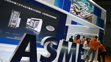

The semiconductor industry has reached a pivotal juncture where the physical limitations of traditional two-dimensional chip architecture are increasingly hindering performance gains. To address these scaling challenges, ASM International, a Dutch-based leader in semiconductor equipment, has officially unveiled its breakthrough XP8 Vertos liquid carbon film technology. This innovation represents a significant shift in how chipmakers address the microscopic voids and structural complexities inherent in modern 3D integrated circuits.
A New Paradigm in Semiconductor Manufacturing
On September 22, ASM International introduced the industry’s first liquid carbon film technology, utilizing an advanced Plasma-Enhanced Chemical Vapor Deposition (PECVD) process. For over two decades, the semiconductor sector has relied on standard carbon-based films to serve as hard masks or sacrificial layers. However, as transistors have shrunk and architectures have evolved into vertical, multi-layered 3D structures, traditional chemical vapor deposition methods have struggled to achieve uniform coverage.
The core problem with legacy technology lies in its inability to coat high-aspect-ratio features evenly. When traditional gas-phase precursors are used, they often fail to penetrate deep into the narrow, high-density trenches of a 3D chip, resulting in uneven surface coverage, residual voids, and structural defects. These imperfections force manufacturers to implement additional, costly, and time-consuming planarization steps—such as Chemical Mechanical Polishing (CMP)—to smooth out the surface before proceeding to the next manufacturing layer.
The XP8 Vertos system solves this by using a liquid-phase precursor that flows into the most intricate crevices of a chip design, filling them from the bottom up. By achieving near-perfect gap-fill capabilities, the technology eliminates the need for redundant processing steps, significantly reducing the risk of wafer defects and lowering the overall cost of production for advanced logic and memory devices.
Chronology of Innovation and Industry Evolution
The development of the XP8 Vertos technology is the culmination of years of R&D at ASM’s facilities, including its major hub in Arizona, USA. The transition from legacy deposition to the liquid-phase approach reflects the broader shift in the semiconductor roadmap:
- 2000s – 2015: The era of standard PECVD carbon films. These methods were highly effective for planar (2D) transistors where surface geometry was relatively simple.
- 2015 – 2022: As FinFET (Fin Field-Effect Transistor) technology became the industry standard, the demand for better aspect-ratio filling grew. Industry players began exploring advanced deposition techniques, but the "void" problem persisted.
- 2023 – Early 2024: Pilot programs and testing phases for liquid-based deposition systems. ASM International focused on refining the stability of the liquid carbon precursor to ensure it could withstand the rigorous heat and plasma requirements of modern fab environments.
- September 2026: The official launch of the XP8 Vertos, marking the first commercially available liquid carbon film solution ready for high-volume manufacturing (HVM).
Supporting Data and Market Context
The launch of the XP8 Vertos comes at a critical moment for the global semiconductor market. According to the Semiconductor Industry Association (SIA), the global semiconductor market is projected to reach an valuation of $1.5 trillion by the end of 2026. This growth is driven by the explosive demand for high-performance computing (HPC), artificial intelligence (AI), and advanced memory modules.
John Neuffer, President and CEO of the SIA, has noted that the robust sales growth across the Americas, the Asia-Pacific region, and China underscores the critical importance of keeping the production pipeline efficient. As chip density increases, the cost of manufacturing "defective" units—chips that fail quality control due to microscopic structural gaps—has become a multi-billion-dollar concern for global foundries.
By utilizing the XP8 Vertos, manufacturers can expect:

- Improved Yield: A significant reduction in "wafer scrap" rates, as the bottom-up fill process prevents internal structural voids.
- Thermal Stability: The material provides enhanced thermal management, which is vital for the power-dense, multi-stacked chip designs required for modern AI processors.
- Process Simplification: The removal of intermediate planarization cycles allows for faster cycle times, reducing the total duration of the fabrication process.
The Engineering Advantage: Why Liquid Carbon?
The primary advantage of the XP8 Vertos lies in its fluid dynamics. When the material is applied, it acts as a liquid that naturally conforms to the complex geometries of a 3D architecture. Once inside the trenches, the plasma process triggers a phase change, hardening the material into a stable, uniform carbon layer.
Unlike traditional vapor-based systems that rely on the diffusion of gas molecules—which can be easily obstructed by the very structures they are trying to coat—the liquid approach ignores these surface tension hurdles. Furthermore, the material is specifically engineered to handle high-angle structures, ensuring that there are no "shadowing" effects where parts of the structure receive less coverage than others.
This is particularly important for the manufacturing of High-Bandwidth Memory (HBM) and next-generation Gate-All-Around (GAA) transistor architectures, where the structural integrity of every individual layer is paramount to the operational speed and power efficiency of the final device.
Broader Implications for the Semiconductor Supply Chain
The introduction of this technology by ASM International is expected to ripple through the semiconductor supply chain. By lowering the barrier to entry for complex 3D chip production, the technology may accelerate the adoption of advanced node designs by smaller foundries that previously found the cost of defect management prohibitive.
However, the industry faces broader challenges. As manufacturing processes become more specialized, the reliance on proprietary equipment like the XP8 Vertos creates a high level of interdependence between equipment suppliers and major chip manufacturers. While this drives innovation, it also necessitates rigorous qualification processes. ASM has noted that the technology is already being implemented in high-volume production, suggesting that major foundry partners have successfully cleared the necessary quality assurance benchmarks.
Furthermore, the environmental impact of chip manufacturing remains a focal point. By reducing the number of processing steps, the XP8 Vertos also contributes to a more sustainable manufacturing cycle. Fewer steps mean less consumption of chemicals, water, and electricity, aligning with the "Green Fab" initiatives currently being pursued by global semiconductor leaders.
Analysis: The Path Ahead
The success of the XP8 Vertos will likely be measured by how quickly it is adopted across different segments of the industry. While its initial application is targeted at high-end logic and memory, the principles of liquid-phase deposition could theoretically be adapted for other thin-film applications in the future.
As the industry pushes toward the "angstrom era"—where features are measured in fractions of a nanometer—the margin for error continues to shrink. Materials and processes that can bridge the gap between design complexity and physical reality will define the next decade of computing power. ASM International’s latest move is not merely a product launch; it is an acknowledgment that the future of computing will be built on our ability to master the smallest, most difficult-to-reach corners of the silicon wafer.
As of late 2026, industry analysts are closely watching to see if competitors will respond with their own liquid-based deposition solutions or if ASM’s early-mover advantage in this space will cement their position as a dominant force in the evolution of 3D semiconductor manufacturing. With the global demand for chips showing no signs of cooling, the ability to produce more complex, more reliable chips at a lower cost remains the single most important competitive advantage in the tech sector.