
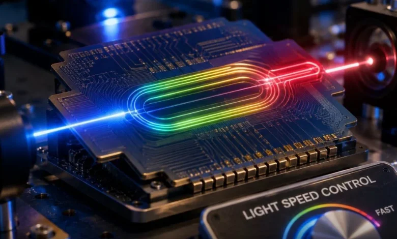
In a significant breakthrough for high-speed telecommunications and data center infrastructure, researchers at Yokohama National University, led by Professor Toshihiko Baba, have developed a compact optical modulator capable of achieving data transmission speeds of up to 200 Gbps. This innovation, dubbed the "Reduced-DSP 200G/λ," utilizes a novel approach that pairs "slow light" technology with integrated electrical balancing, effectively bypassing the physical limitations that have long constrained traditional silicon-based modulators. The findings, published recently in the journal Nature Communications, represent a paradigm shift in how optical data is processed at the chip level, potentially paving the way for the next generation of high-bandwidth artificial intelligence (AI) and cloud computing networks.
The Challenge of Optical Modulation
At the heart of modern data transmission lies the optical modulator—a device that encodes digital data into light signals for transit through fiber-optic networks. Whether transmitting high-definition video, complex AI training datasets, or standard internet traffic, these modulators act as the "gatekeepers" of data speed.
Traditional silicon modulators, while robust, have historically faced a "performance-efficiency trade-off." To increase the interaction between the light and the signal, engineers typically had to make these devices larger or slower. Larger devices, often measuring several millimeters, struggle with high-frequency efficiency, as electrical resistance within the device inherently limits the speed at which it can react. Conversely, shrinking these devices to improve frequency response often degrades the modulation depth, leading to signal loss. For years, the industry has relied on Digital Signal Processing (DSP) to clean up these distorted signals, but DSP chips consume significant power and add complexity to hardware architecture.
The "Slow Light" Solution
The research team at Yokohama National University addressed this dilemma by leveraging photonic crystal waveguides. Unlike standard waveguides that allow light to travel at near-vacuum speeds, these micro-engineered structures contain a series of precisely arranged, microscopic holes. This design forces light to propagate significantly slower than usual.
By slowing down the light, the interaction time between the optical carrier and the electrical signal is substantially increased. This allows for a much larger change in the output light signal even when using a very small electrical voltage. The resulting device is remarkably compact, measuring only 320 micrometers (0.32 mm)—roughly ten times smaller than conventional Mach-Zehnder modulators that typically span 2 to 4 millimeters. The entire footprint of the chip, including electrodes, occupies approximately 0.4 square millimeters.
Chronology of Development and Testing
The path to this 200 Gbps milestone has been characterized by rigorous iterative testing. Early prototypes focused on the fundamental physics of photonic crystal interaction, with the team gradually moving toward the integration of electronic control systems.
- Phase I (Concept): Theoretical modeling of photonic crystal waveguides and the application of slow-light phenomena to optical modulation.
- Phase II (Miniaturization): Integration of the waveguide with CMOS-compatible manufacturing processes to ensure the device could be mass-produced using existing semiconductor foundries.
- Phase III (Performance Testing): Initial tests using on-off keying (OOK) demonstrated a speed of 140 Gbps.
- Phase IV (Signal Optimization): By implementing pulse-amplitude modulation (PAM-4), the team pushed the speed to 180 Gbps without the need for intensive DSP.
- Phase V (The Breakthrough): The addition of an 11-tap electronic receiver allowed the team to stabilize the signal and achieve the final threshold of 200 Gbps.
Technical Specifications and Performance Data
The Reduced-DSP 200G/λ architecture is notable not just for its speed, but for its efficiency. By reducing the reliance on heavy DSP, the chip achieves a lower power consumption profile, which is critical for hyperscale data centers where energy costs and heat dissipation are primary operational concerns.
The device operates across a frequency range that has been significantly expanded, jumping from a 35 GHz baseline to an impressive 80 GHz. This wider bandwidth is what enables the high-throughput transmission. However, the researchers acknowledge that the current prototype faces a hurdle regarding optical insertion loss. The device currently exhibits a loss of 11.7–15.5 dB, which is higher than the 5–7 dB loss observed in traditional commercial modulators. Professor Baba has noted that the team is already exploring the integration of on-chip optical amplifiers to mitigate this, though these remain currently restricted to laboratory testing environments.

Industry Implications and Future Roadmap
The implications of this technology for the AI sector are profound. Modern AI models, such as Large Language Models (LLMs), require massive amounts of data to be shuffled between processors and memory at near-instantaneous speeds. Current interconnects are becoming a bottleneck. A 200 Gbps chip that maintains a small footprint and low energy usage could theoretically double or triple the density of data center interconnects, drastically reducing the energy-per-bit cost of training and running AI models.
Professor Baba and his colleagues are already looking toward the next stage of development: multi-channel integration. The goal is to scale the architecture to support 16 to 32 channels operating simultaneously. If successful, this would allow for aggregate transmission speeds of 3.2 to 6.4 Tbps per device, effectively turning a single chip into a high-capacity backbone for future network switches.
Expert Perspectives and External Context
Industry analysts tracking semiconductor development have long noted that optical interconnects are the "holy grail" for breaking the speed limits of traditional copper-based wiring. While silicon photonics has been a subject of research for decades, the specific approach of using photonic crystals to "slow down" light for modulation represents a creative departure from standard approaches.
"We believe this architecture has the potential to become the foundation for high-efficiency, integrated optical devices in data centers of the future," Professor Baba stated in an interview with Interesting Engineering. By utilizing a CMOS-compatible process, the team has ensured that their invention is not merely a lab curiosity but a viable candidate for industrial mass production.
Broader Impact on Global Telecommunications
As the world moves toward 6G and beyond, the demand for higher bandwidth is inexorable. The "Reduced-DSP" approach provides a blueprint for how to handle the "data tsunami" of the next decade. By moving the burden of signal integrity from power-hungry digital processors to the physical structure of the chip itself, researchers are effectively changing the rules of the game.
The transition from 100G to 400G and 800G Ethernet standards is already underway in global infrastructure. The development of a 200 Gbps-per-lane modulator fits perfectly into the roadmap for high-speed networking, providing a modular, scalable, and energy-efficient building block.
Conclusion and Ongoing Challenges
While the 200 Gbps milestone is a significant achievement, the path to commercialization remains long. The team must address the insertion loss issue to ensure compatibility with standard fiber-optic links without requiring excessive external amplification. Furthermore, ensuring long-term reliability and thermal stability under constant, high-speed usage will be the next frontier for the Yokohama team.
Nonetheless, the successful demonstration of this technology serves as a testament to the power of fundamental material science in solving the biggest engineering problems of the modern age. As data centers continue to grow in complexity and energy demand, innovations that favor efficiency and speed—such as the Reduced-DSP 200G/λ—will be essential to sustaining the digital transformation of the global economy. The collaboration between material engineering and high-speed communications, as demonstrated by this study, will likely remain a focal point for academic and industrial research for years to come.