Researchers from the Chinese Academy of Sciences (CAS) have recently achieved a critical milestone in semiconductor manufacturing by successfully designing a key architecture for sub-3-nanometer chips using legacy Deep Ultraviolet (DUV) lithography equipment. This breakthrough marks a strategic pivot for the Chinese semiconductor industry, which is currently navigating a complex landscape of export controls imposed by the United States and its allies, particularly the Netherlands, which restricts the sale of advanced Extreme Ultraviolet (EUV) lithography systems to Chinese entities.
The development centers on the Gate-All-Around (GAA) transistor architecture, a sophisticated design that addresses the physical limitations inherent in traditional FinFET structures. By optimizing this design for existing DUV technology, Chinese researchers are attempting to bypass the need for EUV machines, which remain the industry standard for high-end sub-5nm chip production.
Contextualizing the Semiconductor War
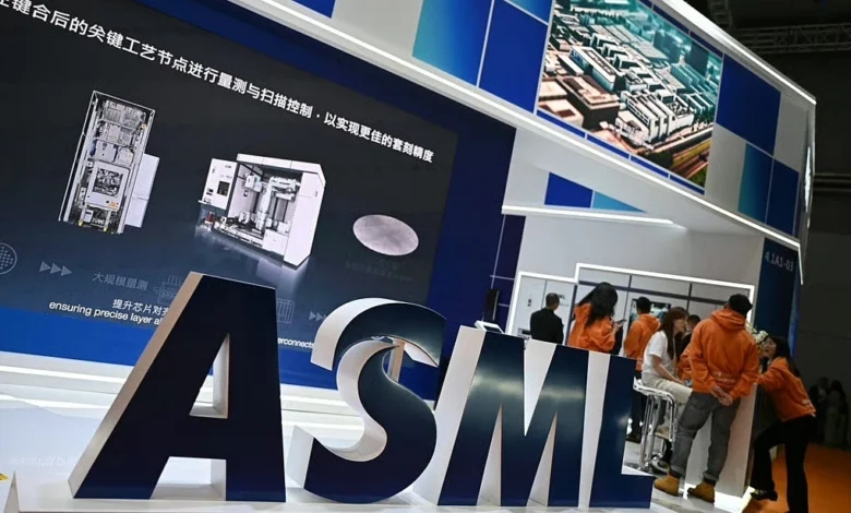
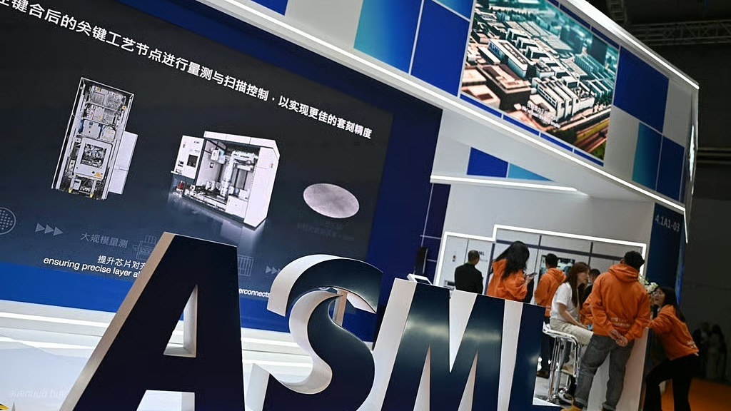
The global semiconductor market has become the primary arena for technological competition between the United States and China. At the heart of this tension lies the EUV lithography machine, manufactured exclusively by the Dutch firm ASML. EUV machines utilize light with a wavelength of 13.5 nanometers, allowing for the extreme precision required to print microscopic features on silicon wafers. In contrast, DUV machines use a 193-nanometer wavelength, which is inherently less precise.
For years, the industry consensus was that sub-3nm nodes were impossible to achieve without EUV technology. However, the combination of U.S. export restrictions—which prevent ASML from selling its most advanced machines to Chinese manufacturers—and the urgent need for domestic self-reliance has forced Chinese institutions to rethink the fundamental physics of chip design.
The Significance of Gate-All-Around (GAA)
The transition from FinFET to GAA is one of the most consequential shifts in modern chip manufacturing. As transistors shrink toward the 3nm threshold, electrical leakage becomes a severe problem, leading to reduced performance and increased heat. FinFET, which stands for Fin Field-Effect Transistor, relies on a three-sided gate to control the flow of current. As the scale decreases, the gate’s ability to "turn off" the current diminishes, causing efficiency losses.
GAA architecture, by contrast, wraps the gate entirely around the channel, providing superior electrostatic control. This allows for higher performance at lower power consumption, which is critical for the next generation of artificial intelligence, high-performance computing (HPC), and advanced mobile processors. While industry giants like Samsung have already implemented GAA in their 3nm processes, and TSMC is transitioning to this architecture for its 2nm nodes, the Chinese research community is now demonstrating that it can potentially achieve this structure using less advanced lithography tools, albeit with significantly more complex multi-patterning techniques.
A Chronology of Technological Resistance
The road to this breakthrough has been paved by several years of intense R&D investment within China:
- 2022–2023: The U.S. government significantly tightened export controls on high-end AI chips and the tools required to make them. ASML was restricted from shipping DUV immersion lithography systems, pushing Chinese firms to focus on optimization and legacy equipment.
- May 2024: Huawei unveiled its "Tau" law strategy, a long-term research initiative aimed at achieving transistor density equivalent to 1.4nm technology by 2031. This served as a signal to the market that the company was looking beyond traditional EUV dependency.
- September 2024: Ye Tianchun of the CAS Institute of Semiconductors confirmed that researchers had successfully validated the GAA architecture using DUV equipment.
- Present Day: The focus has shifted from theoretical design to experimental validation on manufacturing lines. While the laboratory results are promising, the transition to high-volume manufacturing (HVM) remains the most significant hurdle.
Supporting Data and Technical Hurdles
To understand the magnitude of this challenge, one must consider the limitations of DUV multi-patterning. When a lithography machine cannot achieve the necessary resolution in a single pass, engineers use multiple exposures to create a single layer of a chip. This process is exponentially more expensive, time-consuming, and prone to "overlay errors"—where the layers of the chip do not align perfectly.
Current industry analysis suggests that while the CAS achievement is a scientific victory, it does not immediately equate to commercial viability. Yield rates—the percentage of functional chips produced from a single wafer—are the primary metric for economic success. For a 3nm chip to be commercially viable, yields must be high enough to justify the massive R&D and capital expenditure. The CAS research team has acknowledged that they are in the early stages of this transition, with further testing required on actual production lines to determine if the process can be scaled.
Industry and Government Perspectives
The reaction from the broader semiconductor ecosystem has been one of cautious observation. Western analysts note that while China’s progress is impressive, the sheer efficiency gap between EUV-produced chips and DUV-produced chips remains substantial.
"The Chinese strategy is essentially trying to do the work of a surgeon with a scalpel using a kitchen knife," one industry analyst noted. "They can achieve the same goal, but the cost, the time, and the complexity are significantly higher. The question isn’t whether they can make a 3nm chip; the question is whether they can make it at a price point that makes it competitive in the global market."
Domestically, the narrative in China is one of resilience. By leveraging internal design innovation, the government is signaling to the global market that it intends to remain a top-tier player in the semiconductor space, regardless of the limitations placed on imported equipment. This has led to a surge in funding for domestic semiconductor equipment manufacturers like AMEC (Advanced Micro-Fabrication Equipment Inc. China) and Naura Technology.
Broader Implications and Future Outlook
The ability to produce sub-3nm chips using older equipment, if successful at scale, would change the geopolitical calculus of the "chip war." It would suggest that export controls, while effective at slowing progress, may not be capable of halting it entirely.
Furthermore, this development highlights a shift in the global semiconductor hierarchy. The focus is moving away from purely relying on the "best machine" toward "best-in-class architecture." By prioritizing design-level innovations like GAA, China is attempting to maximize the output of the machines it already possesses.
Looking ahead, the next 24 months will be decisive. If Chinese foundries like SMIC (Semiconductor Manufacturing International Corporation) can integrate this new GAA research into their production cycles, they may be able to offer domestic alternatives for advanced chips, reducing their reliance on foreign supply chains. However, the path to commercialization involves overcoming immense logistical hurdles, including the development of advanced packaging techniques and the refinement of chemical materials required for the delicate GAA etching process.
Ultimately, the CAS breakthrough is a testament to the fact that the physics of semiconductor manufacturing is not a closed door. While the global community continues to rely on EUV for high-end production, the ongoing experimentation in China proves that there are multiple pathways to achieving advanced nodes. Whether these pathways prove economically sustainable or merely serve as a temporary bridge to future technological breakthroughs remains to be seen. As the industry advances toward the 2nm node and beyond, the focus will likely remain on how effectively nations can leverage both their intellectual capital and their industrial infrastructure to remain at the cutting edge of the digital age.